
Heisler Semiconductor builds a packaging business around small chip programs
A finished chip is not necessarily ready to go into a device. It still needs a package that connects it to the rest of the electronics and protects it in use. Heisler Semiconductor has built its business around that step, offering assembly and test for customer-supplied chips in quantities that can start with a single prototype.
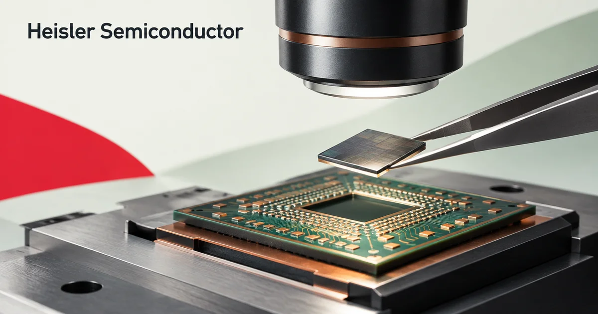
From an early part to a build program
The company operates a process and assembly lab in Halethorpe, Maryland. It does not make the silicon die or sell chips of its own. Instead, it offers packaging engineering, assembly, inspection and test for hardware developers, including programs in medical devices, aerospace and sensors.
Heisler says a program can begin with a first article, move to a pilot and then use the same line for production. That arrangement gives a customer a possible path from an experimental part to later build lots without moving the work to a new packaging provider.
Engineering first, then build lots
For one custom chip-packaging offer, Heisler designs the substrate around the customer’s die and assembles the package. It says it selects an outside vendor to fabricate some laminate substrates, so the service is not entirely confined to its own lab.
The company describes a one-time setup charge for a package family, design and bring-up charges for each die type, and a separate charge for each build lot. Under that offer, repeat lots do not carry another engineering charge; firm prices depend on the customer’s technical data.